The Ultimate3 QRSS/WSPR transmitter kit was produced by QRP Labs from November 2013 to December 2014. In January 2015 QRP Labs produced a new version of the kit, the Ultimate3S. The U3S kit includes an Si5351A synthesiser module kit instead of the previous AD9850 DDS module. The Si5351A synthesiser module kit can be ordered separately from QRP Labs, click to order here.
The Si5351A synthesiser module kit can be plugged directly into an existing Ultimate3 QRSS/WSPR transmitter kit with a firmware version of v3.07 or above. The U3 and U3S kits both use the same firmware. The firmware can automatically detect whether it has a Si5351A synthesiser module kit plugged in, or the old AD9850 DDS module.
HOWEVER, the power output with the Si5351A synthesiser module kit is LOWER than with the AD9850 DDS module. If you want to restore the former power output (and in fact exceed it), this page has modifications that do that. You can argue that the lower power output with the Si5351A synthesiser module is still perfectly acceptable and these modifications to get more power aren't needed. You may agree or disagree. But if you decide to go ahead with hacking up your U3 board, proceed with caution and at your own risk :-)
This modification will also increase the power output if you still use the AD9850 DDS module.
DO NOT think about these modifications if you already own the newer U3S kit: all of these modifications are already standard, in the U3S kit!
There are THREE PARTS to this modification. Only the first part needs to be done to restore the power output. The second and third parts are optional, they can be done to reactly replicate what happens on the U3S PCB, but they aren't necessary. The second and third modifications come TOGETHER; you should not do only one of them. You should also read the second and third sections carefully to understand the consequences.
1) Power Amplifier bias modification
 Firstly, the reason for the low power. The Si5351A has a 3.3V p-p squarewave output, compared to the AD9850 DDS' 5V p-p squarewave output. The gate threshold voltage of the BS170 MOSFET transistor used in the power amplifier has a gate threshold voltage of 3V. The Si5351A does not drive the BS170 gate hard enough past the gate threshold voltage. So the transistor is not switched on fully. The AD9850 DDS' higher 5V squarewave switches the BS170 transistor more "on", resulting in higher power output.
The solution to this is to A.C couple the Si5351A output to the BS170 PA gate, using a capacitor. Then apply a DC bias. This shifts the centre level of the Si5351A squarewave up to near the threshold voltage of the BS170. Then the 3.3V p-p swing is enough to cleanly switch the transistor and produce best power output.
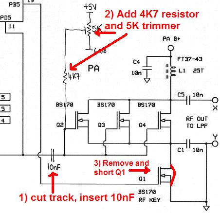
This modification is shown to the right here in this fragment of the circuit diagram of the U3 kit, from the assembly manual.
The power amplifier bias modification is done by cutting the track that leads to the gate of the transistor Q2 (and parallel transistors Q3, Q4). Then insert a coupling capacitor. The diagram shows 10nF, I personally used 0.1uF, it really doesn't matter much.
Secondly, wire a 5K trimmer potentiometer from ground to +5V, and its wiper goes to the Q2 gate via a 4.7K fixed resistor. The actual values aren't very critical. E.g. 10K potentiometer and 10K resistor would be fine too.
It is important to keep all the wires as short as possible. You can also fit a 10nF (etc) capacitor from the trimmer wiper to ground, but I did not find it to be necessary as long as the wiring is kept short. I wired my trimmer potentiometer and resistor right next to the board.
The picture below shows how I made the modifications to the BOTTOM side of my board. Note that my PCB in this photo is my first original U3 kit, with the Revision 1 PCB. The old U3 is pretty well bashed up but still quite functional. That PCB had two tracks missing (design error), and the builder had to add the two wires (mine in the photo are yellow). So ignore those yellow wires. If you have a Rev 2, Rev 3 or Rev 4 PCB the tracks are there on the PCB, and you won't have ever worried about the two wires.
You can click here or on the image for a larger photo.
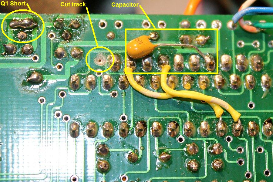
On the PCB you can easily locate the correct via (the little hole that leads a track from the top side of the PCB to the bottom side of the PCB). The via is at the end of the 10-pin header where the DDS or Si5351A board plugs in. Or put another way, it's near pin 17 of the ATmega328 microcontroller. Or, just locate it according to the small yellow circle labeled "cut track" in the photo above :-)
I cut this track really easily, just using a 2mm drill. I didn't even use my dremel drill, I just held the drill bit in my fingers and spun it back and forth on the via until the track broke. You can see the result, in the photo.
Next, just solder a capacitor (e.g. 10nF, 0.1uF, something like that) from the synthesiser output to the Q4 gate (Q2, Q3 gate would be fine too, but Q4 is closer). The synthesiser output pin is the 4'th from the top right of the synthesiser pin header connector, as shown in the photo.
At the top left of the photo you see the label "Q1 Short", this is something I'm going to discuss in the next section. So leave that for now, we'll come back to it.
Now the next photo, shows how I put the resistor and trimmer on the top side of the board. Click here or click the photo, for a full-size version.
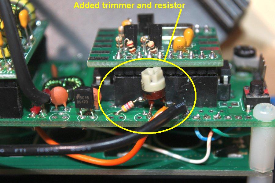
There are many ways this could be done, but this is how I did it in my U3. I have only a single BS170 transistor (Q2), running at 5V. The So there is some space where Q3 and Q4 would go. I soldered the trimmer capacitor ends to +5V and Gnd. My Gnd connection is the right hand pad of Q4 - this is at ground because I removed and shorted my Q1 transistor (See discussion in next section). So you can only do that, if you do the Q1 short. The potentiometer wiper goes via a 4K7 resistor to the Q3 gate pad, in my version.
Anyway however you decide to do it, try to keep the wires short!
Adjustment: before powering up the U3, turn the new trimmer potentiometer all the way anti-clockwise. So that the wiper of the potentiometer is going to be at ground. Depending on how you wired your trimmer, you might be turning clockwise. Just make sure the wiper is positioned at the ground end. Now power up the U3, and set the transmitter up. When transmitting, you can monitor the power output. Then turn the trimmer clockwise and watch the power output increase. At a certain point, it will peak, then start falling again. When you go PAST the peak point, you're just making the poor transistor hotter and hotter (and may fry it completely). So when you find the peak, be on the safe side: back off a bit.
The exact adjustment point does vary slightly depending on band but in general you only need to do this once, the optimum point is not critical and does not vary much by band.
2) Q1 Short (optional mod)
This modificaiton is optional only, it is not necessary for restoring the power output. But if you do it, please also do the THIRD modification described in the following section. Otherwise you may get nasty signals transmitted on 6.75MHz during calibration. I'm including these mods for completeness, because it is there in the Ultimate 3S.
The Q1 BS170 MOSFET transistor is the keying switch. You can get a slight increase in power if you remove Q1 and short it out (as shown top left of the under-board photo, above). In the Ultimate 3S kit there is no keying switch. That space on the PCB has been used for the trimmer. Instead, keying is accomplished by disabling the output of the Si5351A chip, using instructions sent from the microcontroller.
So, if you want to exactly replicate the Ultimate 3S kit then you can remove Q1 and short it out. It produces a small increase in power output too. But, it really isn't necessary - you could also leave the Q1 keying transistor in place quite happily - that's why this modification is OPTIONAL.
But, there's also a PROBLEM with this modification! It needs to be understood. During GPS frequency calibration, the synthesiser output is set to 6.75MHz (Si5351A) or 6.25MHz (AD9850 DDS). The firmware contains a frequency counter that measures this frequency, using the 1 pulse-per-second signal from the GPS. The firmware then adjusts the reference frequency used to calculate and set up the synthesiser (whether Si5351A or AD9850 DDS).
During the GPS frequency calibration, you have to STOP this signal reaching the antenna and being broadcast on 6.75MHz. In the Ultimate3 kit, the keying transistor Q1 is OFF during frequency calibration so the PA is powered down, and the calibration signal isn't broadcast. If you short out Q1, then the PA is enabled!
This is not so much of a problem if you have installed the relay-switched LPF board, because during calibration all the relays are switched off, so nothing reaches the antenna. It's also not a problem if you don't even DO any GPS calibration at all, because you haven't connected a GPS and you calibrate manually.
If you really want to do the Q1 short, and the calibration signal needs to be stopped from reaching your antenna in your case, then you should proceed with the final modification described next.
3) Calibration on the Clk2 synthesiser output
In the Utimate 3S kit the problems described above are entirely avoided by using the Si5351A's Clk2 output. Remember that the Si5351A has THREE independent outputs? Output 0 is routed to the power amplifier (BS170 gate) via the PA bias mod described in section 1 above. All the problems are avoided when Output 0 is disabled during key-up, and Output 2 is separately wired to the microcontrollers frequency counting input, and used for calibration only.
So if you want to do this modification, you have to cut the track leading to pin 11 of the microcontroller. Cut it close to pin 11. Then add a wire from pin 11 of the microcontroller to the Si5351A's Clk2 output. I should add a picture showing this...
The firmware (v3.07) and onwards is neat. At startup, it detects whether you plugged in an Si5351A module or an AD9850 DDS module, and it behaves accordingly. But the firmware also tests the hardware, and works out whether you have the Si5351A's Clk0 or Clk2 output wired to the microcontroller's frequency counter input pin. Then when the kit calibrates, it knows whether to use Clk0 or Clk2 for the calibration.
Summary
Modification 1) restores the power output by a simple bias modification to the U3 PA.
Modifications 2) and 3) would make the U3 exactly a U3S, but are not really necessary just to restore the power output.