This article is also available as a PDF prepared by Edward Karisch on 17-Jul-2018, with page numbers and inverted 'scope trace photos (easier on the printer). DOWNLOAD HERE.
A Japanese translation by Shig JA1XRQ is available, DOWNLOAD HERE and also on Shig's Japanese website about the QCX (THANKS SHIG!)
SEE ALSO: Troubleshooting video
This article is equally applicable to QCX and QCX+ kits, which share the same circuit design and firmware (just a different physical implementation).
I have fixed several QCX kits. The following describes my fault-finding procedure. You can follow these steps too.
Even if your QCX radio works perfectly, signal tracing through the circuit as described on this page, is a very educational experience! You will find you get a greater and deeper understanding of how the QCX works and why. Even *I* find it highly rewarding, and I'm the guy who designed the thing! So - get inside your QCX! Be at one with the circuit! Live the QCX!
Contents
Circuit blocks
Equipment
General checks before starting
Techniques for replacing components
Signal tracing with an oscilloscope
Digital section
LCD all black blocks, or all blank
LCD top row is blocks, bottom row is blank
Unreliable processor boot up
Wrong band selected
Buttons / rotary encoder don't work properly
RECEIVE signal path
Failure to get BPF peak, or a high enough signal strength reading
I-Q and Phase balance fail to how a minimum
Signal generation by the Si5351A
Signal generator injection into the front end
Low Pass Filter fault
T1 transformer
Quadrature Sampling Detector (QSD), IC4
Audio pre-amp, IC5
IC6 and IC7 phase shift circuits
Signal-tracing through the rest of the audio chain
Examples of receiver section faults I have found
TRANSMIT signal path
Current consumption
IC3 the quad NAND gate
Power Amplifier
Low power output
Conclusion
The circuit breaks down into three main blocks, for trouble-shooting purposes: Digital section, Receive signal chain, and transmit signal chain. I handle them one by one. Often you only have a problem in one of these blocks. Throughout the trouble-shooting, you need to keep referring to the circuit diagram, AND the component placement diagram.
This diagram shows the digital section (processor, LCD, buttons, rotary encoder, Si5351A Synthesiser) in the green square at bottom right; the red line shows the transmit signal path, and the blue line shows the receive signal path. Generally speaking, the receive and transmit paths can be debugged by following the signal through from the start to finish of the signal path. Sooner or later we will find something wrong. An incorrect signal, or an absent signal, etc. This will tell us where the fault lies. This is a very methodical approach to the fault-finding and it always works.
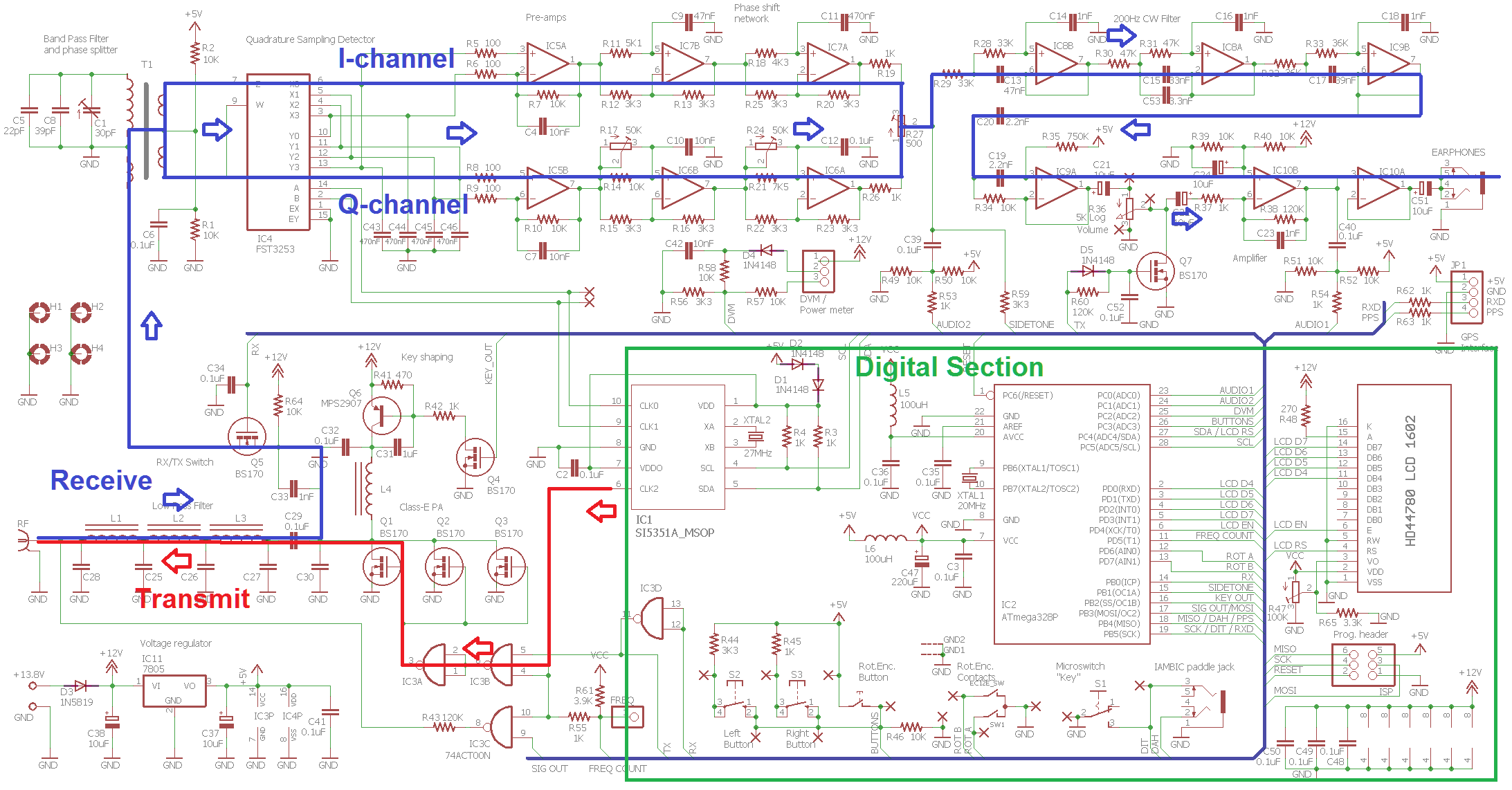
The two most USEFUL diagrams for fault-finding, are the circuit diagram, the parts layout diagram, and the tracks diagram. Remember that on the tracks diagram, BLUE tracks are on the bottom side of the board, and RED tracks are on the top side of the board. These diagrams are in the manual already. But here they are again, just so you have them near at hand.
Click the diagrams to see the larger version; or even better, right-click "Open in new tab" or "Open in new window" etc.


I use an oscilloscope for detecting the signal at each point through the signal path. Some of this trouble-shooting will be quite difficult without an oscilloscope. You can still use a DVM for some measurements (or the internal DVM of the QCX itself, provided you have the digital section working properly). You do not need anything else - the QCX has its own built-in Signal Generator.
General checks before starting
It is worthwhile to check once again, that all of the IC's are properly orientated, with their dimple matching the one on the PCB silkscreen; and examine the PCB carefully, using a bright light and optical magnification (for example, Jeweler's loupe, magnifying glass or USB microscope). Look for any dry joints, solder bridges, any component wires which were snipped off slightly too long and might touch each other and cause short circuits.
There are a lot of parts to solder and it is surprisingly easy to forget to solder a component wire! Or even forget to install a component completely! It has happened time and again. A quite nice trick is to hold the PCB up in front of a bright light. As you look through the board, you will see the sparkle of the light through any holes which have not been soldered. It is a neat trick that really helps find any forgotten joints and it takes only a moment. Don't panic though - remember that band pass filter capacitors C5 and C8 are not always installed (depends on the band).
Also don't panic if you had additional components left over: some capacitors are not used in some band versions of the kit. And sometimes the kit packers make a mistake and put in one too many of a component (which is better than one too few, right?).
Also check that the transistors are installed correctly - they are not all BS170's, there is also one MPS751 (or MPS2907). Make sure that the MPS751 is in the right place (Q6). Check that all the other components are correct too, including:
- Component value
- Orientation of electrolytic capacitors
- Orientation of transistors - the transistor body shape must match the silkscreen; the centre wire of the transistor is bent forward to fit the centre point of the triangle, in the case of the BS170's
- Diode orientation is correct: the stripe on the PCB matches the stripe on the component
- IC dimples line up with the PCB
- All pins of ICs are properly installed in their holes/socket positions (not bent under the chip)
These are preliminary checks, not very exciting, but they are a lot easier than some of the signal tracing that follows. And surprisingly often, you can find the fault just visually like this, without any more complex investigation.
Be sure to read the FAQ and the Modifications pages, to see if any of the problematic symptoms you see on your radio are mentioned there.
Techniques for replacing components
Replacing components should be an absolute last resort! Check EVERYTHING else first! It is easy to suspect a damaged component... but often, the component is not the problem, something else is! Replacing components is not easy, and sometimes you can easily damage the delicate traces on the PCB. Removing components from through-hole plated, double-sided PCBs is not easy. So run through ALL other checks first, to make sure you are certain the component is broken, before trying it!
Removing a resistor or capacitor is normally not so hard, because they have only two wires. I find that by alternately heating one joint and gently pulling, then the other, the component can be "rocked" free of the PCB. If the wires are bent at all on the underside of the board, then start off by straightening them up, so they stand out at right-angles to the PCB. This makes the job a lot easier.
Transistors can also be removed by the same technique, one wire at a time, gradually pushing them this way and that, to gently ease them out bit by bit. Don't be tempted to use too much force, which can lift PCB traces, pads, or even pull out the through-hole plating.
If the component is just installed in the wrong place, and you want to remove it and re-use it, then you need to be very careful not to damage the component as well as the PCB. If the component is broken, then you don't care about damaging it. This can make it easier to remove. For example in the case of a transistor, you can just cut off the transistor wires with a wire cutter. Then remove each wire one at a time, with the soldering iron.
In the case of IC's I don't think you have any choice but to destroy the IC during removal. They have too many legs and you can't easily heat them all at once, or lever the chip out one leg at a time. Surface Mount ICs are easiest to remove and can survive the experience. Some people have hot air techniques where they blast the board with hot air until all the solder joints of the IC are heated, and it just lifts out while everything is molten. This might be Ok if you are salvaging a chip from an old PCB and you don't care much about what happens to the PCB, which can easily get damaged by all the heat. In our case, we do care about the PCB. My method for removing chips (destructively) is, use a very sharp wire-cutter and snip each of the pins right next to the chip body. The chip body can be cut out. Then remove each pin one by one with the soldering iron.
In order to install new components, you will want to clear the solder out of the holes. The holes are all through-hole plated and the solder wants to stay in the hole. But you want to get it out, so you can install the fresh component. There are several ways of doing this. I find that the easiest way is desoldering braid. This is a thin ribbon of copper braid which looks a bit like the outer shield braid of a coax. You put the braid on the hole and hold the soldering iron to it. When the solder melts, it gets sucked up into the braid, out of the hole, just like water into a sponge. That's the theory and it doesn't always work. Don't push too hard with the soldering iron, or hold the soldering iron to the pad too long. Too much heat and it is easy to lift PCB pads.
You can also push something into the hole, while holding the soldering iron to it - something that solder doesn't like to stick to. Some people have reported using sharpened wooden tooth picks for this purpose. I tend to use a thin sewing needle. It often gets stuck in the hole but with care it is possible to gently pull it out, leaving a cleared hole that is suitable for installation of the fresh component.
Where you have accidentally lifted a PCB trace, which can EASILY be done - you can repair the trace by running a thin piece of copper wire along its route. Study the PCB trace diagram in the manual, and make sure that you reconnect the lifted trace to everywhere it is supposed to be connected to. If a hole's through-hole plating comes out, don't worry - again just wire up the connection instead. But be very careful, when replacing lifted traces or through-hole plating, be careful to check on the PCB trace diagram, to see if there are connections on both sides of the PCB. Remember that the job of through-hole-plating is to join the pads on each side of the board. If the pad at the top is connected to a trace, AND the pad on the bottom side is connected to a trace, and the through-hole-plating got removed, then you need to make sure you connect those two sides together. The easiest way in this case is to just apply solder above and below the PCB to connect the wire of the component to the respective pads. It does NOT happen often, because on the QCX, most of the traces are on the lower side of the PCB. But it is something to watch out for.
Signal tracing with an oscilloscope
Use a x10 probe when signal tracing. Some parts of the circuit are high impedance and a x1 probe will load them too much and alter the function.
When using the 'scope probe be very careful that you don't accidentally create short-circuits to nearby component pins or wiring!
Throughout the tracing, do not get too upset if your oscilloscope screen doesn't look exactly like my examples. There are a myriad of possible reasons for this:
- Your oscilloscope is lower quality than mine
- Your oscilloscope is HIGHER quality than mine
- Your 'scope probes are differently adjusted to mine
- Even where you clip the ground lead, will make a difference in the observations...
- Component tolerances and build differences mean amplitudes and waveform shapes may differ
- Etc etc
RF is tricky stuff. Just get the general feel for it. Usually when there is a fault, it will be quite obvious - the results will be VERY different to my examples, not just slightly different.
Digital section
You have GOT to sort this out first, everything depends on the microcontroller operating properly. We cannot go any further, until it is working.
LCD all black blocks, or all blank
If the LCD looks like this, or it looks like that...
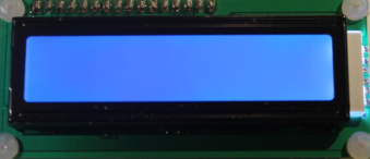
...then most commonly, the problem is simply that the LCD contrast trimmer R47 has not been adjusted. This is a very sensitive adjustment (though easier to adjust from PCB Rev 3 onwards). Do not be tempted to assume that the voltage on the contrast pin of the LCD should match the one shown in the manual - it will vary from LCD to LCD.
If adjusting R47 still doesn't bring visible text to the display, then check with a DVM that you can see the voltage at the LCD contrast pin (pin 3, i.e. 3rd from the left) does vary from 0 to 5V as you turn R47.
If you see the voltage varying correctly from 0 (full anti-clockwise) to 5V (full clockwise) as you turn R47, then there could be a DIFFERENT problem.
Check with a DVM that there are no short-circuits between adjacent LCD pins, or between any LCD pin and Gnd or Vcc. Check for continuity between each LCD pin and the corresponding pin on the processor. You can do this with the board upside down, and the LCD module plugged in.
If ALL of that checks out fine, then there is one more possibility for a blank screen, in firmware versions up to and including 1.00e. In these versions the firmware carries out initialization steps which clear the screen. Then it tries to communicate a command to the Si5351A Synthesizer chip IC1. The commands to IC1 are sent over an I2C serial communication link. If for some reason, the Si5351A does not respond to the command to acknowledge it, then the I2C bus will hang up while infinitely waiting for the response of the Si5351A. The screen will remain blank indefinitely and mislead you into thinking there is a problem with the processor or the screen. So it is worthwhile to check the Si5351A soldering, preferably with a jeweler's loupe or one of the inexpensive USB microscopes, if you have one. Check for solder bridges between pins, mis-soldering, a loose pin, or any other sign that the 10 pins of the Si5351A are not properly connected to the PCB.
Hopefully after all this, you will find the solution to the blank screen.
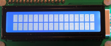
LCD top row is blocks, bottom row is blank
If the screen looks like this...
...then be aware that this is the default state of the LCD module at power-up, if nobody has told it to do anything. It indicates that the processor has not issued any commands to the LCD. This is usually because the processor is not running. If the processor is not present at all, the LCD will look like this too. So though it sounds silly, do check that in your excitement you didn't forget to install the processor ;-) Also check that the processor is installed correctly - the dimple at one end of the processor must face to the right side, where it will match up with the dimple indicated on the PCB silkscreen (white print).
If the processor is present and orientated correctly, the next thing to check for is that all the pins are properly inserted into the socket. We did have one or two cases where the 28-pin socket was missing a pin. A manufacturing defect. Presumably you would have noticed that during soldering - but just check again now too. When the chips arrive from the factory, the legs are slightly splayed outwards. It is necessary to gently squeeze them inwards so that they fit in the socket. It is quite easy to push the chip in the socket, and not notice that one of its legs has bent inwards rather than properly going into the socket. So check that all the pins are nice and straight, and all are properly in their sockets. If any pins of the processor are not properly connecting with the socket - then this cause the processor to fail to start; it can also cause many other kinds of failure too, depending on which pin it is, that is not connecting.
A common cause of the processor failing to start up, IF your board is a Rev 1 or Rev 2 PCB, is described by this simple modification described here, to ensure reliable processor startup. On the Rev 3 PCB, this modification is already included as standard, so this paragraph doesn't apply. Whenever I am fault-finding a QCX, if it is a Rev 1 or 2 PCB, I always implement this modification first, before anything else.
If that doesn't help, you can also check that the 20MHz crystal is oscillating. This can be done with an oscilloscope with x10 probe at IC2 pins 9 and 10 (NOT a x1 probe, which will load the crystal oscillator pins of the processor too much). You could also listen for the signal at around 20MHz, with a general coverage receiver. But bear in mind it will likely be several kHz off frequency, so tune around for it.
Right at the END, you can suspect that the processor is faulty. This does happen but is rare. My GENERAL RULE is that we intuitively always want to suspect defective components, rather than our own mistakes in assembly; but when we find out what is wrong, it usually turns out to be OUR MISTAKE, not a defective component! We want to make this work, not massage our ego... so always suspect defective components ONLY as a last resort when all other avenues of investigation are exhausted.
When the processor boots up, the first thing you will see, is the question about which band to select. You have to turn the rotary encoder to select the band you built the kit for. It is important to select the correct band, NOT to choose the wrong band then tune to the one you really want, using the rotary encoder. This is because the firmware adjusts the Si5351A commands for the chosen band, in the configuration which generates 90-degree quadrature oscillator signals; but this configuration must be altered for very large frequency changes, such as to another band.
If you chose the wrong band, the best way to recover the situation is to undertake a factory reset using menu item 7.8, then turn the power off, and on again, and this time select the correct band.
Buttons / rotary encoder don't work properly
If you discover that you cannot operate the buttons correctly, or the rotary encoder does not work as expected - then this can occur also due to the lack of the reliable processor start-up modification, on a Rev 1 / Rev 2 PCB. See above. It is important to realize that even if the processor appears to have booted up properly, and is writing to the LCD etc., in some cases the unreliable start-up issue can mean that the Analogue-to-Digital Converter (ADC) subsystem does not work properly. Reading the three buttons depends on the ADC. If the ADC is not working, then the buttons will be mis-read, or not read at all. So again, it pays to implement the modification.
RECEIVE signal path
Failure to get BPF peak, or a high enough signal strength reading
The best way to check that the receiver is working, is to use menu item "8.7 Peak BPF". If the displayed signal strength shows at least 8 or 9 in the display top right corner, and if you hear a loud tone in the earphones (do NOT put them in your ears while you do this!), then the BPF peaking has probably worked well. This signal strength is independent of volume control setting. If the signal strength is less than 7, or if there is no peak, then it is necessary to investigate further.
If the peak in BPF occurs with the trimmer capacitor fully open, or fully closed, then it is necessary to add or remove turns from the T1 transformer. This is described in detail in the manual, so please refer to the relevant section.
I-Q and Phase balance fail to show a minimum
Now check the unwanted sideband alignments:
- 8.8 I-Q bal.
- 8.9 Phase Lo
- 8.10 Phase Hi
Note that the displayed signal strength level unfortunately depends on the volume control setting, because the ADC for these weak signal (unwanted sideband) measurements is tapped from the signal path AFTER the gain control. It would have been nice if this was not the case, but it would have required another op-amp.
If the displayed signal strength is 12 or 13, then this is too HIGH, it means the ADC is saturated and it will not show anything meaningful. So turn down the volume a bit.
If the displayed signal strength is 1 or 2, then the signal strength bar will jump around too much because you will mostly be measuring noise rather than the signal - so, turn the volume up a bit.
Once you have the signal strength display of a reasonable magnitude, you should be able to make the adjustments as described in the relevant manual sections. If you do not get the right signal strengths or if you do not manage to see any minimum, which should be quite easily seen, then it is time to investigate further with some proper signal tracing through the receive path. If there is a fault in the I or Q channels, then there will be no unwanted sideband cancellation, and no minimums can be found. So a fault somewhere in the I or Q signal paths is the usual cause of not finding a minimum.
Signal generation by the Si5351A
When in the menu "8.7 Peak BPF", we can use this to trace the signal generator output, which is Clk2 of the Si5351A IC1, all the way through the Receive path to the earphones. The Clk2 output of IC1 feeds into the IC3c NAND gate, at IC3 pin 10. During signal generation mode, to inject the signal into the receivers input (right at the RF connector of the transceiver), the NAND gate is enabled by the processor signal "SIG OUT". Then the 5V peak-peak squarewave coming out of IC3 pin 8 is routed to the RF connector through the 120K resistor R43.
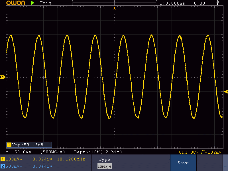
This is what it looks like on my oscilloscope, at IC3 pin 8. Note the horizontal speed 50ns/div, and the signal frequency measurement on the 'scope, 10.120MHz - this was on a 30m QCX kit. Don't worry too much that is is not a precise-looking square wave. 'Scope probes, long wires, 'scope bandwidth... long story, out of the scope (pun not intended) of this article.
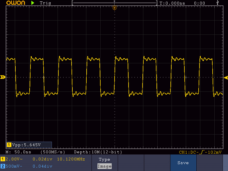
If you do NOT see a nice 5V peak-peak squarewave here on IC3 pin 8, then you have to trace back further to see why you do not have a signal from the Si5351A Synthesiser chip (IC1). Check on pin 10 of IC3. You should see a 3.3V peak-peak squarewave. IC3 pin 10 is connected directly to IC1 pin 6 (Clk2 output of the Si5351A). If you do not see this signal then check for track discontinuities, check for short-circuits to ground, or to nearby pins.
EXAMPLE: I had one repair case where the IC3 pin 10 was at 3.3V permanently, regardless of what was done with the processor. Upon inspection of IC1 (Si5351A) with a jeweler's loupe, I could see a very tiny whisker of solder lying between IC1 pin 6 (Clk2 output) and IC1 pin 7 (+3.3V). This was shorting Clk2 to the Si5351A's 3.3V supply, and explains why there was no oscillator output signal from Clk2. I could easily remove the solder whisker just by briefly touching IC1 pin 6 with the soldering iron. Problem solved!
Note that this problem of Clk2 shorting to +3.3V would have caused a lot of problems on transmit. On key-down, a high current would flow from +12V through Q6, through L4, and through the BS170 MOSFETS Q1, Q2 and Q3. Everything would get very hot and eventually something would fry.
Signal generator injection into the front end
The size of this resistor (120K) has been chosen so that when in the "8.7 Peak BPF" menu, the ADC is not overloaded, and a meaningful adjustment can be made. However, 120K series resistor into a 50-ohm load, which is approximately what the impedance of the transceiver's RF in/out is, means the 5V signal is reduced by a factor of 2,400 approx. This is a 2mV signal and it gets further attenuated by losses in the BPF and the mixer... and so it is way WAY too small to be able to view the signals on an oscilloscope.
In order to be able to trace an actual signal through the first few stages of the receiver, I first bypass R43 by temporarily soldering a 330-ohm resistor in parallel. This is easy to do on the bottom side of the PCB. Be careful to find R43, at the correct place on the PCB, using the layout diagram - it is right next to the BNC connector. Now the attenuation factor is only about 1/6th. It doesn't have to be 330-ohms. I wouldn't go below 220-ohms which will load IC3 too much and probably make the signal a bit too big; but 220-ohms, 270-ohms, 330-ohms, 470-ohms, 560-ohms... anything like this should be good enough. The later stages of the receiver will be massively overloaded. But we don't care - for now we just want to be able to see the signal as we trace it through the front end of the receiver.
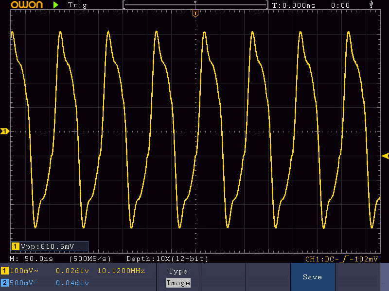
The signal strength will be a bit more or less depending on whether or not you have a dummy load connected. It doesn't matter. We are only interested at this stage in seeing a signal which is strong enough that we can trace it through the first few stages. Here's the 0.8V peak-peak signal that I see with the 'scope probe right at the BNC connector.
Check with the oscilloscope for a good strong signal at the drains of the BS170 MOSFET's Q1, Q2, Q3. Or alternatively at the final pad of the LPF inductor L3 (the pad closest to the microprocessor). What you are checking here is that the signal is coming through the Low Pass Filter (LPF) correctly. If it is not, we have to investigate why.
The most common fault is failure to properly solder to the wire of the toroids in the LPF, which are L1, L2, L3. If the enamel insulation is not properly burnt or scraped off, the solder will not make an electrical connection between the wire and the PCB. So no current can flow. This is easy to check, using a DVM to check for DC continuity through the inductors.
The same thing applies equally to L4, and the windings of T1.
The transformer T1 has multiple functions. It is used for band-pass filtering, and to split the phase of the incoming received signal into two paths, with 180-degree phase difference. These are fed to the double-balanced quadrature sampling detector (IC4).
Bear in mind the circuit diagram fragment and the section of the PCB layout diagram:
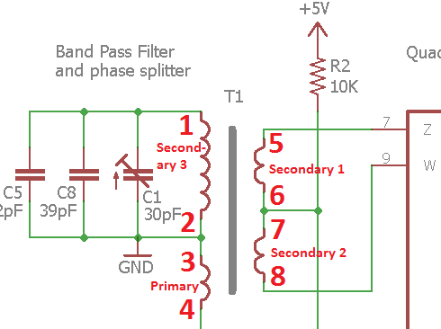
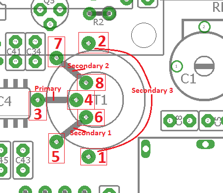
Now we can check at the top end of the long winding of the T1 transformer. Since this long winding and the trimmer capacitor act as a band pass filter, you can see that we see a nice sinewave now. This is labelled "1" in the diagrams above. It is the point shown by the arrow, in this photograph:
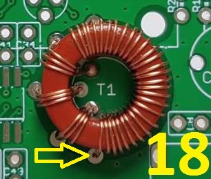
Note that the amplitude of the sinewave seen at this resonant tank circuit does change when you adjust trimmer capacitor C1. Try it, just to prove it and to check. This is not an accurate way to adjust the band pass filter, because the 'scope probe itself also loads the resonant circuit. So it is not a substitute for using the configuration menu item. But it's nice to see that the theory holds true in practice. And it also verifies that the BPF circuit is working properly - which is what this fault-finding is all about, after all.
If you can't adjust the amplitude with the trimmer capacitor, then check that the trimmer capacitor is correctly installed and soldered; and check that it was not broken during the installation; or the delicate plastic melted by over-heating.
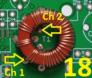
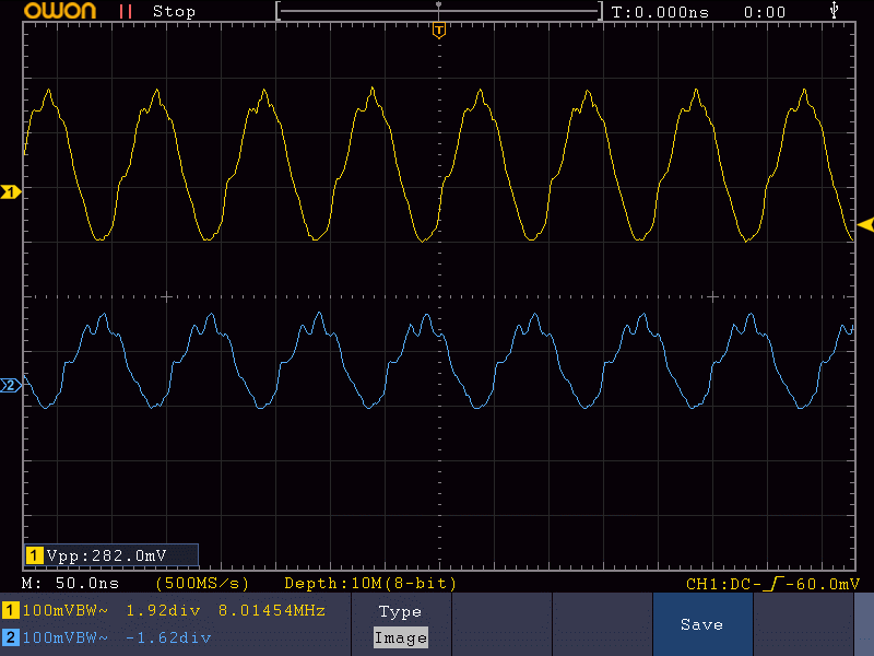
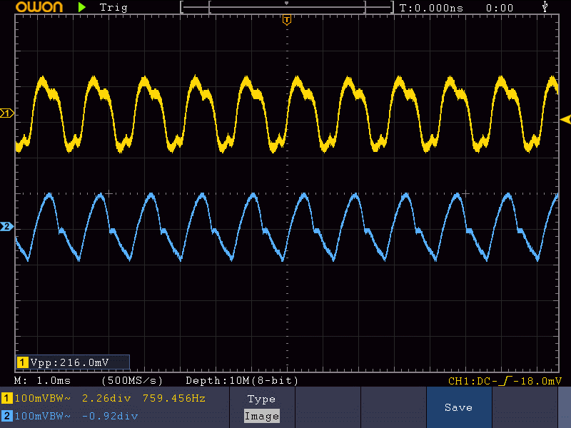
Next we can check at the outputs of the secondary windings of T1. These are the windings which feed pin 7 and pin 9 of the Quadrature Sampling Detector (QSD), IC4. Now although the amplitude is a bit weaker now we can still observe it quite well, even after the BPF adds some loss, and after the phase-splitter formed by these two transformer windings and loaded by the Quadrature Sampling Detector's sampling capacitors C43-C46.
This is a bit tricky to see, because there is also an audio frequency component leaking back through the mixer, and other unpleasantness. If you have a Digital Storage Oscilloscope you can switch on the 20MHz Bandwidth limiting on both channels, and you can use it in Single-shot rather than continuous Run mode - then you can grab a screenshot like this one below and see what is going on. The upper trace (Ch 1) is IC4 pin 7, the lower trace (Ch 2) is IC4 pin 9.
The oscilloscope probes for Ch 1 and Ch 2 were connected to the points indicated by the yellow arrows. It is easier to hold the 'scope probes on these points, than on the pins of IC4 itself, since the IC is Surface Mount and a bit small.
Note the difference in amplitude, which is not very important, this is a Double-Balanced QSD, and everything cancels itself out, all sins disappear, and even if they didn't, we still have an amplitude balance adjustment later, which is R27, the I-Q balance trimmer potentiometer.
Note the 180-degree phase difference between the two channels, which IS important. Critical in fact, to the design of the mixer, which is a Double-Balanced QSD. If the two input signals to the QSD do not have a 180-degree phase difference, then it is highly likely that you have mis-wired T1. Remember that the manual prescribes a method for winding T1 which is designed to ensure that all the windings are in the correct "sense" and the ends of the windings go in the correct PCB holes, to ensure correct phasing of the T1 secondaries. So if you don't see 180-degree phase difference, go back and check T1 again.
Quadrature Sampling Detector (QSD), IC4
Next we can actually observe the audio frequency signals, with 700Hz frequency, at the four outputs of the Quadrature Sampling Detector circuit around IC4. Note that from now on, I have changed the horizontal speed to 1ms/division, for suitable observation of 700Hz audio frequency signals. The signals are a bit wide, because superimposed on the audio frequency, is still a component of the local oscillator frequency. This is filtered out in the pre-amp stages by capacitors C4 and C7.
The following traces are taken from resistor R5 (Ch 1) and resistor R9 (Ch 2), at their junction with the Quadrature Sampling Detector's sampling capacitors (these are C43-C46, refer to the circuit diagram). If you have assembled the PCB in the recommended way, putting the body of the resistor on the side where the silkscreen has a circle drawn (refer to layout diagram in the manual), then the side of the resistors R5, R6, R8 and R9 nearest the top of the board, will be the long wire of the resistor; it makes a neat hook to attach the x10 'scope probe to!
You should check the waveform on each of R5, R6, R8, R9, which is equivalent to saying, across each of the capacitors C43-C46. You are expecting to see 700Hz audio frequency signals. Yes they all have a slightly different amplitude, but you want them to be approximately equal; and yes, the waveforms are not really nice sinewaves... just ignore that too, for now. Just make sure that all four signals are present and look very approximately similar.
If any or all of these four QSD outputs do not have a signal, then we have to check the circuit around the QSD.
The first thing to do is to check the Clk0 and Clk1 outputs of the Si5351A Synthesiser. These have a test pin soldered in the PCB (if you followed the assembly manual accurately). You can easily check there with an oscilloscope and should see the 10.120MHz squarewave (for 30m; for other bands, of course it will be the selected alignment frequency for that band). If you do not see either of Clk0 or Clk1 then you have to examine the Si5351A for any issues with soldering, such as short-circuits, solder blobs (too much solder), poor connections (too little solder). Many of these defects will be possible to resolve, with careful soldering.
If you see Clk0 and Clk1, but you are still missing one of these four phase outputs, or if one looks very wrong, then you should inspect carefully the FST3253 multiplexer chip, IC4. Again inspect under a bright light and optical magnification, look for solder bridges or other defects, as for the Si5351A. The Si5351A and the FST3253 were soldered by SMD machines in the factory, but just like humans, even these machines are not 100% perfect.
Also check that the capacitor and resistance values are correct, and all these components are correctly installed and soldered. I once made the mistake of soldering the four resistors where the four capacitors should go, and the four capacitors where the four resistors should go. I have no idea why I am even admitting this in public...
Now we will check the audio pre-amp, IC5. The following trace shows IC5 pin 1 (upper trace, Ch 1) and IC5 pin 7 (upper trace, Ch 2). These are the famous "I" and "Q" channels. Notice that I have changed the vertical scale to 5V/division. The waveforms are horrendously distorted. Why? Simply because these pre-amps have 36dB of gain. The small input signal results in a large output signal, after 36dB of gain... and the output amplitude cannot be represented accurately by the operational amplifier, whose outputs cannot stray beyond its supply voltage rails (0V and 12V in my case). So you get this nasty clipping.
I'm using 500us/horizontal division now - but either 500us or 1ms is fine for looking at 700Hz audio frequencies.
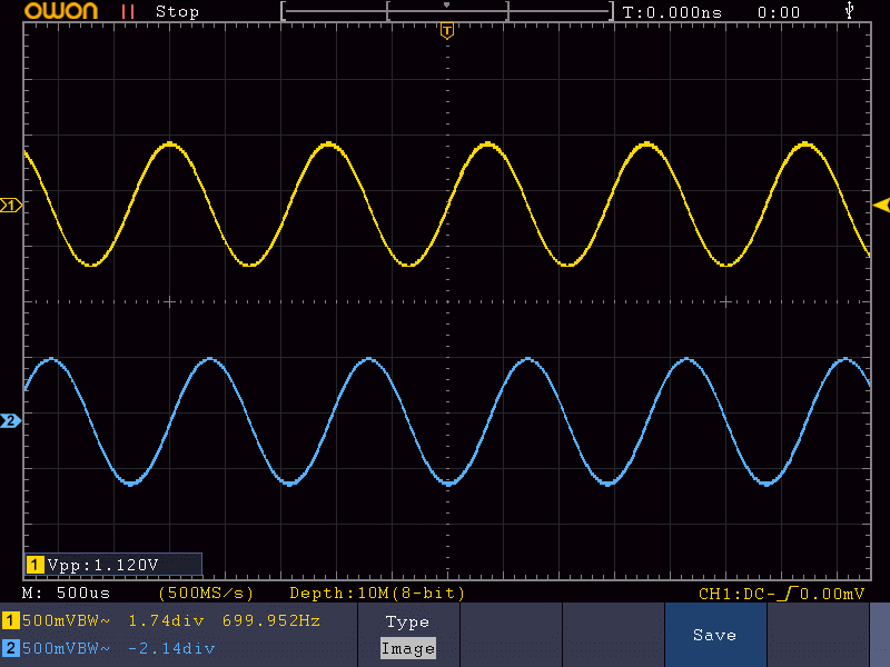
Since we have now come to a stage of the receiver where we have some gain applied, we need to now reduce the amplitude of the signal injected into the input. I removed the 330-ohm resistor in parallel with R43 and instead, soldered in a 10K resistor.
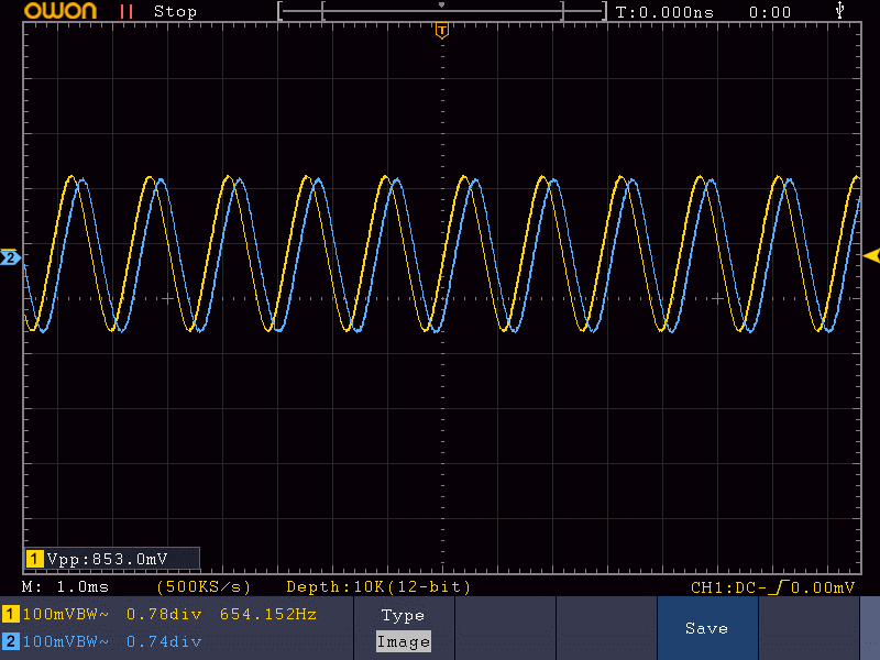
Now the vertical scale on the 'scope is 500mV/division and you can see the 1.1V peak-peak amplitude is a nice 700Hz sinewave without any visibly evident distortion. Again the I channel (IC5 pin 1) is top ('scope channel 1) and the Q channel (IC5 pin 7) is bottom ('scope channel 2).
Now if I shift the Channel 2 trace ("Q" channel) to overlay the Channel 1 trace ("I" channel) you can very clearly see the 90-degree phase offset between the I and Q channels. The amplitude is also very similar.
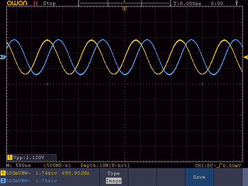
Now, if you see signals that are wildly different from this, or not with the right phase offset, or not approximately equal amplitude - then worry about IC5 and its surrounding circuits. This is the area of the circuit to examine carefully for faults, dry joints, incorrect component values, solder bridges, etc.
IC6 and IC7 phase shift circuits
Now it is time to check the 90-degree phase shift circuits, the four op-amps made by IC7 (I-channel) and IC6 (Q-channel).
My simple technique is to look at pin 1 and pin 7 of each of the chips IC6 and IC7. At each of these outputs I am expecting to see a clean 700Hz sinewave and the amplitude should be practically the same as in the former 'scope screenshot. The audio phase shift circuits are supposed to have a gain of 1.
NOTE: that the only exception to this, is the case where 1K and 3.3K are swapped. This was the case in some early batch kits, due to an error on the silkscreen. The silkscreen wasn't changed in later batches, but the assembly manual was altered to match the PCB silkscreen. If you built your kit using a manual version 1.00 to 1.07, then you have the swapped 1K and 3.3K resistors, R19 and R25. If you built your kit using manual version 1.08 or above (published 23-Oct-2017) then R19 and R25 are not swapped. These two resistors R19 and R25 are next to each other on the board. R25 is closest to the IC7 chip body near pin 8 and it is supposed to be 3.3K. R19 is supposed to be 1K and is next to the R27 I-Q balance trimmer potentiometer. If these two are swapped, it is nothing to worry about. It means that the gain of IC7a will be increased, so it no longer has unity gain. By good fortune (or otherwise, since it masked the problem for some time), if R25 is 1K and the IC7a gain is increased, then R19 being 3.3K largely compensates for this unexpected gain, cancelling out the problem. Remaining amplitude imbalances can be adjusted out using R27. So the swapped resistors are NO PROBLEM, I am just mentioning it because if you saw the sinewave at IC7A pin 1 looking 3x as big as the one at IC6A pin 1, then this is normal IF you have the swapped resistors. No panic.
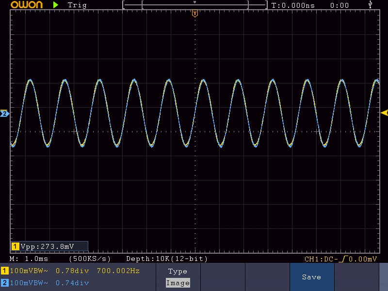
This screenshot below shows the signals at IC7a pin 1, and IC6a pin 1. These are the outputs of the I and Q channels, after the 90-degree phase shift has been applied. Remember that the kit is in menu item "8.7 Peak BPF" where the signal generator is injecting a tone 700Hz higher than the receiver oscillator, resulting in 700Hz beat note. This is on the WANTED sideband, so we expect that after the 90-degree phase shift, these two signals will be IN-phase. In the screenshot below, you can see that the signals have similar amplitude but are displaced - this is a phase error.
Now you can easily adjust the phase shift adjustments R17 and R24, to bring the two channels into phase. As you turn R17 and R24 you will see the two sinewaves line up on top of each other. This is only a rough adjustment, the oscilloscope won't show tiny phase errors closely enough to get really good unwanted sideband cancellation. This should be done only using the menu items 8.8, 8.9, 8.10. I only mention it here because it is useful to check these things during fault-finding.
Signal-tracing through the rest of the audio chain
I didn't take any more screenshots of the process. You get the idea, hopefully. Just keep going, from left to right across the circuit diagram, checking the output of each op-amp - which is either pin 1 or pin 7 of the dual-op-amp chips IC5, 6, 7, 8, 9 and 10. Use a 330-ohm (or similar) resistor temporarily soldered across R43 in the first few stages, where the signal level is low. Change it to 10K to check IC5, IC6, IC7 outputs (since 36dB of gain has been applied by the pre-amps made from IC5 op-amps). Then remove the 10K resistor completely for checking IC8, IC9 and IC10 outputs. If the volume control is too high (too far clockwise) then you will see the output of IC10b and IC10a is a distorted sinewave or clipped (reaching near the voltage rails). This is normal, it just means that you are over-driving the amplifiers. Even with a 120K signal, the 2mV input injection is a MASSIVE signal compared to the weak signals well below 1uV that the radio can detect. Just reduce the volume.
As you move from left to right, if there is a fault in the Receiver, then at some point you will find the error. The signal will disappear, or the amplitude will be wrong, or the signal distorted, or some other problem. In these cases, check the relevant components near that op-amp carefully, for soldering errors: dry joints, solder bridges, solder blobs, etc. Some thin solder whiskers can cause a short, and be nearly invisible - so use a bright light and optical magnification if possible. You can use a DVM to check for shorts between nearby components, or shorts to ground, shorts to the supply voltage.
Using these techniques, I have a 100% success rate so far in finding faults in the receiver chain and getting them working.
Examples of receiver section faults I have found
1) There was no signal at R9. But there was a signal across the relevant Quadrature Sampling Detector capacitor C45. I took a closer look visually, at the components nearby. It was easy to see that the wire of resistor R9 was broken (it looked as though it had been cut!). It was easy to apply a blob of solder to fix it.
2) One time the signal just stopped abruptly. All the components looked fine, the soldering looked fine. I could not find any short circuits. Eventually, using the DVM to check for continuity between component leads which were supposed to be connected, I found one which wasn't. With the jeweler's loupe I eventually found a tiny track fault next to a component pad. The track was disconnected from the pad, right at the pad. The break was so tiny it was hard to see even with a jewler's loupe. The only way to find it was by this signal tracing method, and the DVM for continuity. Once found, easily fixed.
3) In one case, there was no audio output. When the radio was in mode "8.7 Peak BPF" the screen bar showed only 1 or 2 (top right hand corner). I used the above signal tracing method and I found that the signal stopped at IC9B, which had no output. Visually checking the related components showed that the wire of R33 (36K resistor) had become detached, right at the resistor body. Since it was the end of the resistor at the PCB, it was hard to see. I replaced the resistor and all was well. Note that if you do not have the correct value component, you can make one up by series or parallel combinations. For example, 36K is not a common value, but you could use a 33K and a 3.3K in series if you have them, these are much more common values.
4) There was very low audio output, and when you turned up the volume, there was a loud squeal as the audio amplifiers self-oscillated. Signal tracing revealed a strong (about 1V peak-peak) triangular-wave oscillation, at a frequency of around 240kHz (not stable), at IC6 outputs (both output pins 1 and 7). Inspection revealed no obvious flaws and I decided there must be a problem with IC6, and I decided to replace it. It was VERY difficult to remove, because it is sandwiched right between the multi-turn trimmer resistors R17 and R24. Eventually I did manage it (albeit with a one damaged trace and one removed through-hole plating, which had to be repaired). I installed a new LM4562 op-amp... and... SAME PROBLEM! Finally after some head-scratching and experiment, I realized the problem! R24 was right at the end of its travel, with a resistance of zero ohms. The output of the op-amp IC6B was effectively connected straight to the 0.1uF capacitor C12, and it did NOT like that - the result was the unstable oscillation. All that was necessary to resolve it was just to turn R24 slightly so its resistance was no longer zero, and the op-amp started behaving! This is a great example of me violating my own rule, about not replacing components until the last possible moment! Very often you find in the end, that the component was NOT the problem.
TRANSMIT signal path
The transmit side is easier to trace, just because it is shorter. The components are more likely to be broken, because there are high powers involved, which might have fried components.
If you have no transmit power output, first check that you do not have "Practice mode" enabled in the configuration menu! In recent firmware versions when Practice Mode is enabled a 'P' appears in the top line of the display, to the right of the operating frequency. (Thanks Gordon KI7MWA for this suggested addition).
The first clue to a problem with the transmit side, is often high current consumption. Refer to the current consumption chart in the manual. For example at 12V supply, in receive you can expect a current consumption of about 120mA. If it is significantly more than this, maybe you have a problem with the PA. If it is a lot more, then you probably can see smoke rising from some of the components (transistors) in your transmit section at the top right area of the PCB. It is very useful to use a power supply with current metering, and keep an eye on the current consumption to make sure it is in the expected range.
I start with IC3. This is a quad NAND logic gate, a 74ACT00. The 74ACT family was chosen because the logic "1" threshold is 2.4 (old classic 7400-series TTL level) and therefore it is perfect for being driven by the 3.3V peak-peak square-wave from the Si5351A Synthesizer IC1's Clk2 output.
With the radio in ordinary RECEIVE mode, you can check the voltages at all the pins of IC3. I know, you cannot even REACH IC3 because the LCD is in the way. You can temporarily un-plug the LCD while the radio is in receive mode. As long as you don't press any buttons you can be sure that the radio will continue working, even without the LCD. The processor only talks at the LCD, it does not look or wait for any response. The voltages on the IC3 pins MUST be as follows, in receive. Remember that pin 1 is at the top left, when the chip is orientated with its dimple pointing upwards. For convenience, this table is arranged consistently with the pin lay-out:
| 1: +5V | 14: +5V |
| 2: +5V | 13: +5V |
| 3: 0V | 12: +5V |
| 4: 0V | 11: 0V |
| 5: 0V | 10: 0V |
| 6: +5V | 9: 0V |
| 7: 0V | 8: +5V |
The voltages do not have to be EXACTLY 0V and 5V, but they should be very close. Measure the voltage at pin 14, this is the 5V supply voltage from the voltage regulator IC11. It should be close to 5V. All the other voltages should also be close to 5V, or close to 0V, as per the table.
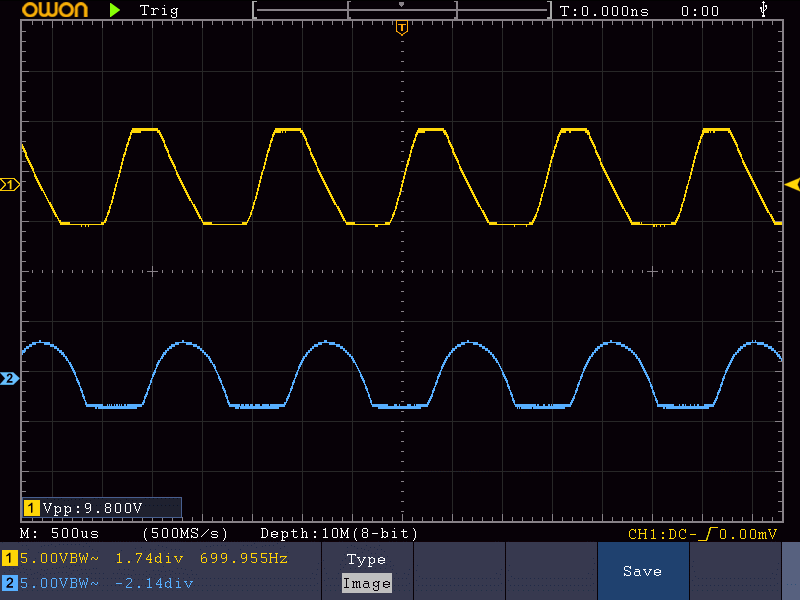
When the radio is in TRANSMIT mode, the NAND gates are changed, so as to allow the signal generated by IC1 (Si5351A) Clk2 output to be gated through to the PA transistors. The 74ACT00 is also supposed to produce 5V peak-peak at its output, so that the three BS170 MOSFETS Q1, Q2 and Q3 are saturated in the ON/OFF states, this is important for achieving high efficiency Class-E operation. The voltages will now be as follows:
| 1: 5V squarewave | 14: +5V |
| 2: 5V squarewave | 13: 0V |
| 3: 5V squarewave | 12: 0V |
| 4: 3.3V squarewave | 11: +5V |
| 5: +5V | 10: 3.3V squarewave |
| 6: 5V squarewave | 9: 0V |
| 7: 0V | 8: +5V |
Again the 0V and 5V in this chart, should measure pretty close to 0V and 5V. 4.8V, 4.9... fine... 0.1V, fine... but if you see 1V somewhere, then that is a reason to worry.
This is an example of what you should see at IC3 pin 3, the 5V peak-peak squarewave. You can ignore the "ringing" appearance, the imperfections on this trace - blame the 'scope probe, the ground clip, the oscilloscope's limited bandwidth, whatever. That's another topic entirely. You can also usually ignore it when the pins which should be 0V and +5V show a bit of RF on the oscilloscope trace - again probes and ground clips can pick up this sort of thing easily.
If you do NOT have an oscilloscope, and you just look at these chip pins with a DVM, then you may see that a 3.3V peak-peak squarewave is measured as its average on a DVM, i.e. 1.65V (or thereabouts); and a 5V peak-peak squarewave measures something around 2.5V.
EXAMPLE: I had one QCX radio for repair, where the current consumption, in receive, was 260mA. IC3 felt very warm to touch. I measured the voltages at the pins, in receive mode... and I saw some strange voltages e.g. 1.4V which were not near to 0V or 5V. In transmit mode, the 3.3V peak-peak squarewave was present at pins 4 and 10, but there was no 5V peak-peak signal at the relevant pins. Reluctantly, and ever-mindful of my own rule about not assuming a component is defective until the last possible moment, and wary of the fact this IC3 has 14 pins and is going to be a bear to remove - I decided I had to replace it. It wasn't as hard to remove it as I had expected (see above section on techniques for replacing broken components), and desoldering braid sucked most of the solder out of the holes. One trace got damaged and I repaired it. The current consumption after the change returned to normal, around 110-120mA, and the voltages looked normal again.
EXAMPLE 2: Another case I heard of, had no Clk2 signal. This turned out to be some kind of corruption of the Microcontroller configuration, and it was cured by doing a Factory Reset - refer to manual for how to do a Factory Reset. (Thanks Gordon KI7MWA for this suggested addition).
The output Low Pass Filter (LPF) continuity has already been covered further up this page. If your receiver is working properly, you will have verified that the signal is coming correctly through the LPF. The only thing in between IC3 pin 3 and the LPF is the Power Amplifier! IC3 pin 3 is connected directly to the gates of Q1, Q2 and Q3 which are the BS170 transistors of the Power Amplifier.
Make sure a 50-ohm dummy load is connected to the QCX transceiver RF output, when testing the Power Amplifier!
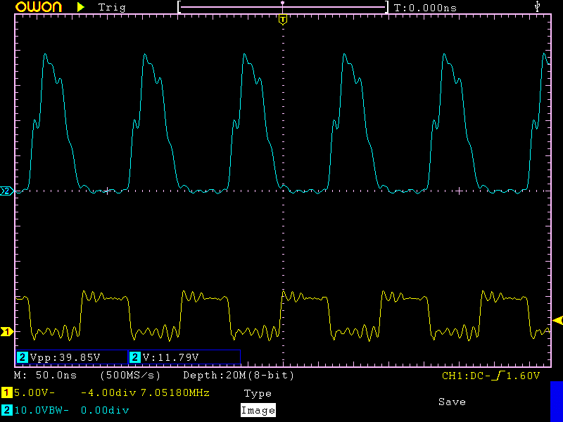
Now check the drains of Q1, Q2 and Q3. Refer to the parts layout diagram and the track diagram. You can see a big fat trace on the bottom of the board, which connects each of the drains of the BS170s and connects them to C29. From there, the signal goes to the Low Pass Filter. On key-down you should see a huge ugly signal, that looks like the upper trace in this 'scope screenshot. The lower trace shows the signal at the BS170 gates (the old 5V peak-peak squarewave from IC3 pin 3). Again please ignore "ringing", and unpleasant notches on the trace (explanation: 'scope probes, long ground clip wires, 'scope limited bandwidth, you name it, let's not debate it right now). Note the vertical scale 10V/div and that this ugly drain waveform is 40V peak-peak. The Low Pass Filter will subsequently sort this out and make a beautiful pure sinewave out of it.
If you do not see this big ugly signal at the BS170 drains, the next thing to investigate is where the BS170's get their supply power from. Check L4 carefully, a common mistake with toroids is the failure to burn/scrape away the enamel coating on the wire, resulting in no electrical connection. No electrical connection means no voltage will reach the PA, and no power output will result. It is easy to check for DC continuity between the pads of L4. Be sure to touch the DVM probes on the pads, NOT on the wires themselves. If there is no continuity, apply the soldering iron and some more solder and hold it there for maybe 10 seconds, to burn off the enamel. Some people prefer scraping, I prefer burning.
Now check at the collector of Q6 (MPS751/NPS2907 PNP transistor that performs keying envelope shaping). This is the junction of Q6 collector and L4. On key-down you should see a DC voltage here (with some superimposed, for sure). The DC voltage will be your supply voltage minus a volt or so - which is lost in the reverse polarity protection diode D3 at the transceiver's supply voltage input, and some voltage lost across Q6 itself. If there is no high DC voltage at the Q6 collector, you have to suspect that Q6 might have failed. You also need to check Q4, which is another BS170 MOSFET. On key-down, you should see approximately 5V DC on its gate; and the source should drop to near ground. Check also the other components around Q6, make sure that you installed the right components, and that they are all properly soldered, without shorts or solder bridges etc.
The manual contains charts of power output vs supply voltage. Remember to take into account that you will lose 0.4V or so across the reverse polarity protection diode D3. The chart voltage is the voltage AFTER this diode. The voltage drop across the diode will be around 0.3-0.4V.
If you see power output, but you think it is too low - then here's what to check.
Firstly, did you calculate the power output correctly? To accurately measure power output on an oscilloscope you MUST have a 50-ohm dummy load connected. Then the peak-peak voltage of the sinewave can be read from the oscilloscope. The power in Watts, is the peak-peak voltage squared, divided by 400. For example, if you see a 37V peak-peak sinewave, this is 37 * 37 / 400 = 3.4W.
You CANNOT reliably measure power in this way, if you have your QCX connected to an antenna. Most power meters will be measuring the peak RF voltage (or RMS voltage) and converting this to power, using the above formula. These power meters necessarily assume that you are measuring a pure sinewave. This is also why you CANNOT measure the power at the drains of the BS170s (Q1, Q2, Q3) in the power amplifier! The signal here is FAR from a clean sinewave. The calculation is invalid, since the calculation assumes a sinewave. So, ONLY measure power across a 50-ohm dummy load such as the QRP Labs dummy load kit, and only measure the power output at the proper RF output connector of the transceiver, after it has been filtered into a nice sinewave by the Low Pass Filter.
If you are using an external power meter, remember that often power meter accuracy is not great. Due to the Square function in the formula for conversion from volts to watts, a small difference in peak voltage measurement is translated into a larger difference in calculated output power.
If you are using the internal RF power meter facility in the QCX, then remember that this too is not very precise. It is a reasonable indication, for debugging purposes, but it is not a precision instrument.
Note also that to get 5W power output does require a 15 or 16V supply voltage. You can see this from the power vs supply voltage curves in the manual.
Finally if you really think your power output is a lot lower than you expected - then you can look at the windings on L1, L2 and L3, the Low Pass Filter toroids. There can be variation in component value due to manufacturing tolerances, and variation in inductance values due to winding style and other factors. First check that you wound the correct number of turns for your band. Remember that what counts as one "turn" is every time the wire passes through the toroid ring's hole. Count the turns again to make sure you got the correct number.
If you have the facility to measure inductance then you can do so - but remember that a lot of inductance meters are not all that accurate either, and this is a topic which always generates a lot of discussion when it arises.
Simply removing a couple of turns from each of L1, L2 and L3 is usually sufficient to raise the filter cut-off, if it was too low - and you should notice a power output increase.
Conclusion
With a highly methodical approach to the fault-finding, to step through one stage at a time through the receive, then the transmit, signal paths - it is always possible to find the fault(s).
This page will be updated in future with more examples of faults, as and when they arise.
In my opinion, the signal tracing is a worthy exercise in itself, even if you have a completed and working QCX - because it is very educational, you really get a deeper understanding (and love) for your QCX when you see all these signals throughout the transceiver.